When rebuilding the Echo you can use a TL7524 as a replacement for both, the output buffer 74HC374 and the DAC ZN426. Just ground the /CE-input of the TL7524 and connect the /WR-input of the TL7524 to the DFF,Clk signal in the original circuit.
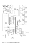
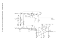
The circuit diagram is split into an analog part and a digital
part. Click on the following thumbnails to get the corresponding
circuit diagrams in DIN A4 postscript format.
|
|
|
| Digital part. | Analog part. |
Note, that this is my first use of Eagle-light. So, please excuse graphical imperfections in the circuit diagrams.
The next figure shows the timing diagram.
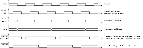
For the description of the timing diagram, we assume that the sampling frequency of the ADC is 10kHz. As mentioned above, this frequency can be up-scaled as much as the decreasing conversation quality of the DAC admits.
With the help of two D-Flipflops two 20kHz clock-signals Clk and ClkD are derived from some 40kHz-square signal. Thereby, ClkD is a 90°-delayed version of Clk.
The counter is driven by the Clk signal. The bits CT1 to CT15 of the counter are used for the address bus of the memory. That means that the memory address is incremented with a frequency of 10kHz -- half the frequency of Clk.
In my first design of the timing diagram I planned some delay between the low-high transition of /M,CE and the low-high transition of /ADC,RD. That complicated the circuit diagram. Frank Dachselt checked the timing diagram for me. He suggested to use the same low-high transition for /ADC,RD and /M,CE. That works since the memory is very fast and from /M,CE to /ADC,RD there is some logic that introduces some gate delay. That simplified the design quite a bit. Thank you, Frank!
Active Butherworth filters of third order are used as anti-aliasing filter and as reconstruction filter (steep filters are needed because of the relatively low oversampling).
The active anti-aliasing filter also works as the microphone pre-amplifier. The pre-amplification level can be adjusted by the potentiometer R3.
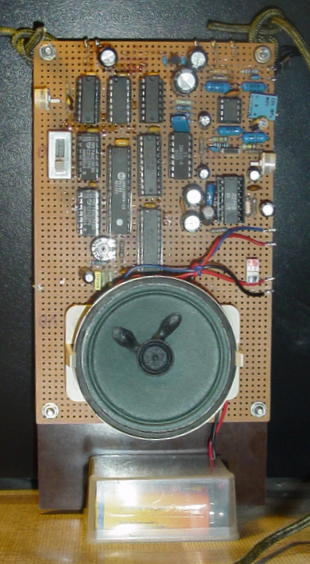
Thomas Falk helped me with testing of the circuit in a lab at the electronical department of TU-Dresden. Since I left my magnification glasses at home I could not see the solder pads. So, he also made some necessary changes for me. Thank you, Thomas!
|